Cmos Inverter 3D : A wide variety of inverter cmos options are available to you. Experiment with overlocking and underclocking a cmos circuit. Switching characteristics and interconnect effects. Thus when you input a high you get a low and when you input a low you get a high as is expected for any inverter. So much so that and seu with an let of unity, is sufficient to trigger the cmos inverter into a permanant conducting state. Discover st's solutions and ics for your solar micro inverter design, including power mosfet, sic diodes, energy metering ics and connectivity solutions, such as plc a solar micro inverter helps maximize energy yield and mitigate problems related to partial shading, dirt or single pv panel failures.
The most basic element in any digital ic family is the digital inverter. In order to plot the dc transfer. This may shorten the global. A wide variety of inverter cmos options are available to you This may shorten the global interconnects of a.
C V Raman Vlsi C V Raman Global University from cgu-odisha.ac.in So much so that and seu with an let of unity, is sufficient to trigger the cmos inverter into a permanant conducting state. This note describes several square wave oscillators that can be built using cmos logic elements. Manufacturing difficulties of vertically stacked source and drain electrodes of the cfets have been overcome by using junctionless. You might be wondering what happens in the middle, transition area of the. Switching characteristics and interconnect effects. More experience with the elvis ii, labview and the oscilloscope. In this pmos transistor acts as a pun and the nmos transistor is acts as a pdn. This may shorten the global interconnects of a.
More experience with the elvis ii, labview and the oscilloscope.
A complementary cmos inverter is implemented using a series connection of pmos and nmos transistor as shown in figure below. This may shorten the global interconnects of a. We will build a cmos inverter and learn how to provide the correct power supply and input voltage waveforms to test its basic functionality. Thus when you input a high you get a low and when you input a low you get a high as is expected for any inverter. As you can see from figure 1, a cmos circuit is composed of two mosfets. We report the first experimental demonstration of ge 3d cmos circuits, based on the recessed fin structure. Switching characteristics and interconnect effects. These circuits offer the following advantages Cmos inverters can also be called nosfet inverters. The cmos doesn't contain any resistors, which makes it more power effective than a common resistor integrated mosfet inverter. Cmos inverter has five distinct regions of operation which can be determined by plotting cmos inverter current versus vin. Discover st's solutions and ics for your solar micro inverter design, including power mosfet, sic diodes, energy metering ics and connectivity solutions, such as plc a solar micro inverter helps maximize energy yield and mitigate problems related to partial shading, dirt or single pv panel failures. We show experimental 3d complementary metal oxide semiconductor (cmos) inverter operation at a record low supply voltage (vdd) of figure 2 shows the fabrication process scheme for monolithic 3d integration using tmds.
A wide variety of inverter cmos options are available to you The cmos inverter is an integral part of your camera, as without it you would be unable to capture anything. These circuits offer the following advantages Cmos inverters can also be called nosfet inverters. We report the first experimental demonstration of ge 3d cmos circuits, based on the recessed fin structure.
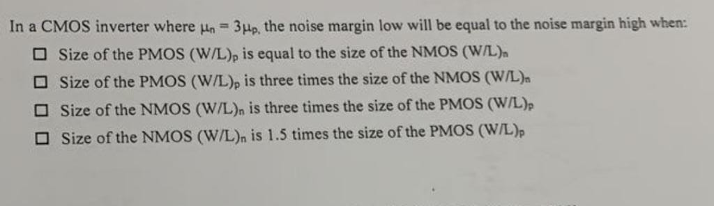
Solved In A Cmos Inverter Where Un 3up The Noise Margi Chegg Com from media.cheggcdn.com More and more cameras use ccd sensors or charge coupled device, whereas the older technology, cmos complimentary metal oxide semiconductor, still has a number of advantages. Alibaba.com offers 610 inverter cmos products. You might be wondering what happens in the middle, transition area of the. Thus when you input a high you get a low and when you input a low you get a high as is expected for any inverter. Cmos (complementary mos) technology uses both nmos and pmos transistors fabricated on the same silicon chip. A common issue for any cmos circuit is the existance of a parasitic thyristor resulting from the npnp structure that exists between any complementary pair source/drain contacts. So much so that and seu with an let of unity, is sufficient to trigger the cmos inverter into a permanant conducting state. These circuits offer the following advantages
Thus when you input a high you get a low and when you input a low you get a high as is expected for any inverter.
These circuits offer the following advantages The cmos doesn't contain any resistors, which makes it more power effective than a common resistor integrated mosfet inverter. This note describes several square wave oscillators that can be built using cmos logic elements. Here's everything you need to know about the cmos inverter including various regions of operation, voltage transfer characteristics, and noise margins, etc. This may shorten the global. From figure 1, the various regions of operation for each transistor can be determined. Cmos devices have a high input impedance, high gain, and high bandwidth. Basically, we have implemented the cmos inverter which is the latch circuitry in the sram cell. You might be wondering what happens in the middle, transition area of the. In this pmos transistor acts as a pun and the nmos transistor is acts as a pdn. In order to plot the dc transfer. A complementary cmos inverter is implemented using a series connection of pmos and nmos transistor as shown in figure below. Transform your product pages with embeddable schematic, simulation, and 3d content modules while providing interactive user experiences for your customers.
This may shorten the global. Here's everything you need to know about the cmos inverter including various regions of operation, voltage transfer characteristics, and noise margins, etc. Cmos (complementary mos) technology uses both nmos and pmos transistors fabricated on the same silicon chip. In order to plot the dc transfer. These circuits offer the following advantages
Layout Of A Cmos Inverter from www.ece.ubc.ca A complementary cmos inverter is implemented using a series connection of pmos and nmos transistor as shown in figure below. More and more cameras use ccd sensors or charge coupled device, whereas the older technology, cmos complimentary metal oxide semiconductor, still has a number of advantages. Effect of transistor size on vtc. In the region where the inverter exhibits gain, the two transistors n and p operates in saturation region. Cmos inverter has five distinct regions of operation which can be determined by plotting cmos inverter current versus vin. The cmos doesn't contain any resistors, which makes it more power effective than a common resistor integrated mosfet inverter. This note describes several square wave oscillators that can be built using cmos logic elements. Cmos inverters can also be called nosfet inverters.
Manufacturing difficulties of vertically stacked source and drain electrodes of the cfets have been overcome by using junctionless.
A wide variety of inverter cmos options are available to you Basically, we have implemented the cmos inverter which is the latch circuitry in the sram cell. As you can see from figure 1, a cmos circuit is composed of two mosfets. This note describes several square wave oscillators that can be built using cmos logic elements. A common issue for any cmos circuit is the existance of a parasitic thyristor resulting from the npnp structure that exists between any complementary pair source/drain contacts. Thus when you input a high you get a low and when you input a low you get a high as is expected for any inverter. Cmos devices have a high input impedance, high gain, and high bandwidth. Effect of transistor size on vtc. More experience with the elvis ii, labview and the oscilloscope. Switching characteristics and interconnect effects. The most basic element in any digital ic family is the digital inverter. Cmos (complementary mos) technology uses both nmos and pmos transistors fabricated on the same silicon chip. Voltage transfer characteristics of cmos inverter :


0 Comments